JTAG接口PCB设计要点
1、 Keep JTAG traces as short as possible.
2、 Either galvanically isolate JTAG ground from offboard
equipment or make sure that the PCB and the
off-board equipment share a common ground.
3、 Add a 3–5 kΩ pull-up resistor to the JTAG interface’s
TCK pin to reduce susceptibility to EMI.
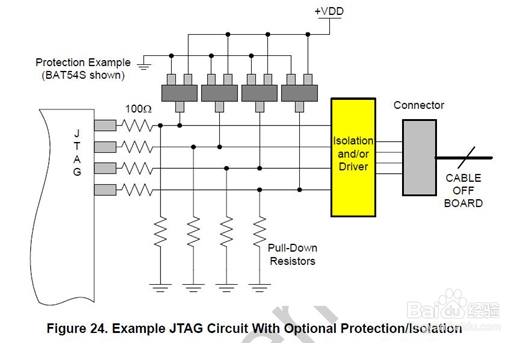
4、 In noisy systems, add pull-down or pull-up resistors
to every JTAG signal.
5、 Place small series resistance on JTAG traces that
are routed to external connectors.
4.3.2. The JTAG Interface
Because JTAG signals have only a weak on-chip pull-up
resistance and are not deglitched, signal traces are particularly
susceptible to noise coupling and EMI. To
reduce EMI sensitivity, JTAG traces should be kept as
short as possible. If the PCB is not galvanically isolated
from the off-board equipment (see 5. "Isolation And Protection"
on page 11), the PCB and equipment must
share a common ground, which can be established by
connecting a pin of the JTAG header to the PCB ground
plane.
The JTAG signals can be made more immune to noise
by adding some passive circuitry. External pull-up or
pull-down resistors can be added to aid the relatively
weak on-chip pull-ups.
Most applications will be sufficiently protected by adding
a 3–5 kΩ pull-up resistor to the TCK signal. If the device
is to be used in a particularly noisy environment, all
JTAG signals should have strong external pull-ups or
pull-down circuits to digital ground. Please note that
placing a pull-down resistor on TCK will make your
hardware incompatible with the USB Debug adapter.
Capacitive ringing across long JTAG cables can cause
communication difficulties. Placing www.faqikan.com a
small series resistance
on JTAG signals dampens this ringing and
improve performance.
Silicon Laboratories MCU target boards use a 5x2
header. Figure 11 shows a circuit diagram for the
header, along with connections for a JTAG device.